Navigation
Part 1

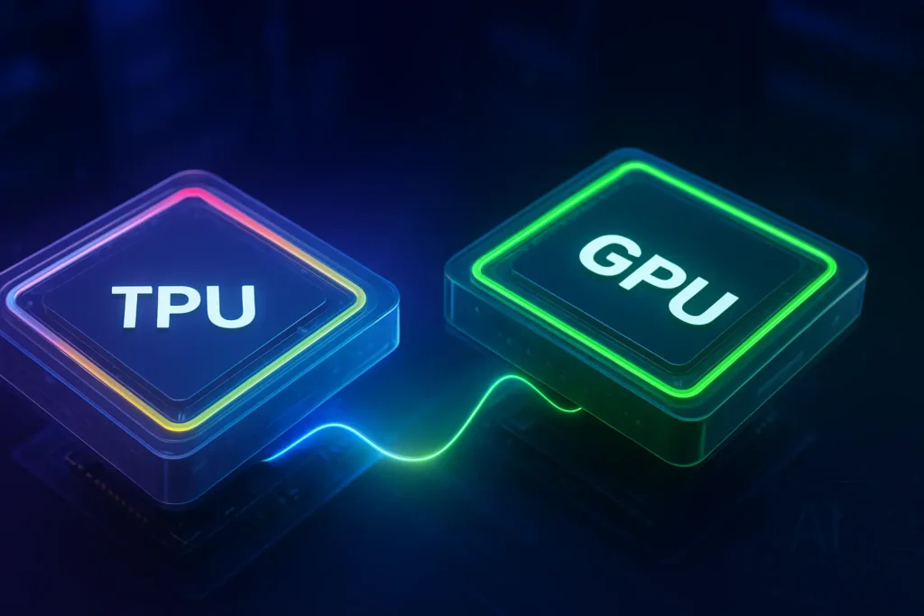
In the world of AI acceleration, Google’s Tensor Processing Units (TPUs) stand out as specialized powerhouses. Designed to accelerate machine learning workloads, TPUs have become a critical component in large-scale deep learning tasks — often outperforming traditional GPUs and CPUs in raw throughput for specific tasks.
In this article explore what TPUs are, how they differ from CPUs and GPUs, and how the latest TPU generations stack up against NVIDIA’s top-tier GPUs like the H100 and H200.
GPU and TPU: What’s the Difference?
To understand what makes a TPU unique, we need to look at how it compares to its sibling in the computing world.
- GPU (Graphics Processing Unit):
A parallel processor originally designed for rendering graphics. Today, GPUs are widely used for machine learning, scientific computing, and simulations. Their architecture makes them ideal for matrix-heavy operations like those found in deep learning. - TPU (Tensor Processing Unit):
An application-specific integrated circuit (ASIC) built by Google specifically for accelerating machine learning workloads — especially those based on matrix computations. TPUs shine in training and inference of deep learning models, particularly in frameworks like TensorFlow and JAX.
How Does a GPU Work?
A GPU (Graphics Processing Unit) is a massively parallel processor originally built for rendering images and video, but now widely used for AI, scientific computing, and simulations.
Instead of a few powerful cores like a CPU, a GPU contains thousands of smaller, efficient cores organized into groups called Streaming Multiprocessors (SMs). These cores carry out the same operation on many different pieces of data at once, a parallel processing approach known as Single Instruction, Multiple Threads (SIMT), an approach similar to Single Instruction, Multiple Data (SIMD), but each thread can have its own control flow.
For AI workloads, GPUs use Tensor Cores (specialized units for matrix math) alongside traditional CUDA cores. Data flows from high-bandwidth memory (HBM or GDDR) into these compute units, where operations like matrix multiplication, convolution, and vector arithmetic are processed in parallel. The results are then written back to memory for the next stage.
This parallel design makes GPUs extremely fast for workloads that can be broken into many small, independent calculations — like the matrix operations at the heart of deep learning.
How Does a TPU Work?
At the heart of a TPU is its ability to perform high-throughput matrix multiplication, the cornerstone of neural network computation. Unlike GPUs, which rely on general-purpose cores and broad memory hierarchies, TPUs are built around systolic arrays — optimized circuits that perform multiply-accumulate (MAC) operations in a tightly choreographed, energy-efficient flow
Data flows through the TPU in stages:
- The host streams data into an infeed queue.
- The TPU loads it into high-bandwidth memory (HBM) along with model parameters.
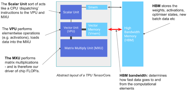
- The Matrix Multiplication Unit (MXU) performs the MAC operations inside the systolic array.
- The final results are placed into an outfeed queue for the host to retrieve.
Because matrix multiplications happen entirely within the array once data is loaded, TPUs can achieve very high computational throughput for training and inference.
What’s more, TPUs rely on reduced precision formats like bfloat16 (brain floating point), which offer a sweet spot between performance and numerical stability in deep learning models. This enables TPUs to deliver extremely high FLOPS (floating point operations per second) without the memory and power burden of full 32-bit or 64-bit precision.

TPU Architecture
A TPU chip contains one or more TensorCores, each made up of a Matrix-Multiply Unit (MXU), a vector unit, and a scalar unit. The MXU, arranged as a systolic array — 256×256 in TPU v6e or 128×128 in earlier versions — delivers most of the compute power, performing 16,000 multiply–accumulate operations per cycle with bfloat16 inputs and FP32 accumulation. The vector unit handles operations like activations and softmax, while the scalar unit manages control flow and memory addressing.
A TPU Pod is a contiguous set of TPUs grouped together over a specialized network, with chips grouped into slices linked by high-speed Inter-Chip Interconnects (ICI). For large workloads, multislice mode connects several slices via both ICI and the Data Center Network (DCN), enabling training across far more TPU cores than a single slice can provide. The number of TPU chips in a TPU Pod is dependent on the TPU version.
TPU Versions and GPU Equivalents
The following comparisons are made using Google’s standard 8-chip TPU configurations, which are among the smallest topologies available for TPUs. Larger topologies (e.g., 64- or 256-chip pods) deliver even higher performance and scale — but these 8-chip systems already rival some of the most powerful GPU setups available.
TPU Version (8-chip topology) | TPU BFLOAT16 TFLOPS | TPU Memory (HBM) | Closest GPU Equivalent | # of GPU Chips | GPU Memory (Total) | GPU BFLOAT16 TFLOPS |
| TPU v5e-8 | 1,576 TFLOPS | 128 GB | 1 x H200 SXM | 1 x H200 GPU | 141 GB | 1,979 TFLOPS |
| TPU v5p-8 | 3,672 TFLOPS | 760 GB HBM2e | 1× H100 NVL | 2 x H100 GPUs | 188 GB (2×94 GB) | 3,341 (2 x 1,671) TFLOPS |
| TPU v6e-8 | 7,344 TFLOPS | 256 GB HBM | 2× H100 NVL | 4 x H100 GPUs | 376 GB (2×188 GB) | 6,682 ( 2 x 3,341) TFLOPS |
| 1 x H200 NVL | 2 x H200 GPUs | 282 GB (2 x 141 GB) | 3,342 TFLOPS |
Recent TPU generations from Google (v5e, v5p, v6e) deliver massive compute power for AI training and inference, especially in cloud environments. Here’s how they compare to NVIDIA’s most advanced GPUs in terms of bfloat16 performance, memory, and overall compute capacity:
- TPU v5e-8 offers 1,576 TFLOPS with 128 GB HBM, roughly comparable to a single NVIDIA H200 GPU (1,979 TFLOPS, 141 GB) for the full 8-chip system. It’s ideal for efficient inference and fine-tuning.
- TPU v5p-8 delivers 3,672 TFLOPS and a massive 760 GB of memory, making it a strong match for a dual H100 NVL setup (3,341 TFLOPS, 188 GB). It’s suited for full-scale model training.
- TPU v6e-8, Google’s most advanced TPU yet, reaches 7,344 TFLOPS with 256 GB HBM, closely rivaling a quad-H100 NVL system (6,682 TFLOPS, 376 GB). It can also be compared to a dual H200 NVL configuration (3,342 TFLOPS × 2).
In essence, TPUs pack more memory per system and deliver extremely high throughput for AI workloads, often surpassing equivalent GPU setups in raw TFLOPS — especially when leveraging Google Cloud’s optimized TPU infrastructure.
When Should You Use a TPU?
TPUs are especially useful when:
- You’re training or fine-tuning large-scale transformer models (e.g., LLMs).
- You’re already using TensorFlow or JAX, which have native TPU support.
- You need maximum performance per dollar/watt for model training.
- You want to run inference at scale with latency and cost-efficiency.
However, if your workflow requires mixed-precision FP8 support, advanced graphics rendering, or tight integration with CUDA-based software, a GPU (especially NVIDIA’s H100 or H200) may still be the better choice.
TPU vs GPU: Which One’s Better?
The answer is: it depends on what you’re optimizing for. For flexibility, GPU wins as it supports a wider range of applications and frameworks. For cost-effective, large-scale ML training and inference, TPU can be more efficient, especially when accessed via Google Cloud. For availability, GPUs are easier to acquire and integrate into on-prem or multi-cloud workflows. For throughput per watt, TPUs generally lead, thanks to their domain-specific design.
Keep Reading
AI That Works Like You. Get Started Today!
Get in Touch to Access Your Free Demo


